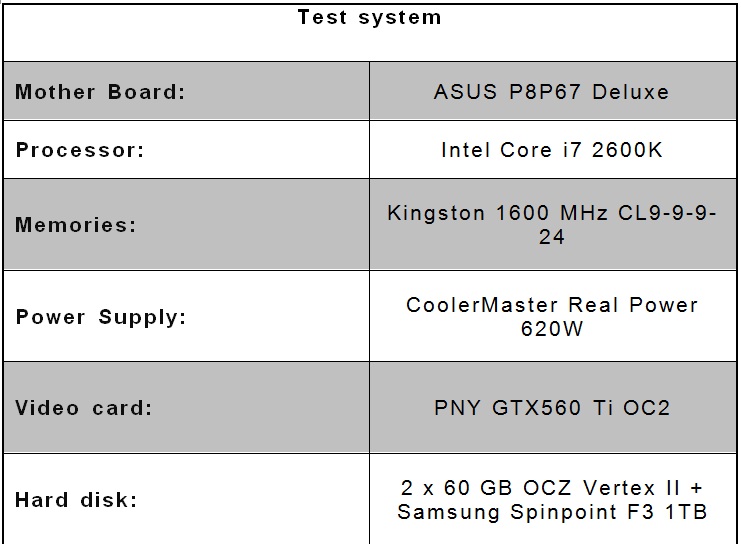
Test System and Test Methodology
For testing we used the following configuration:
We performed the tests by setting the base clock of our CPU to the default frequency (100 MHz), so we initially proceeded to perform our tests by simply editing the RAM divisors on our motherboard. We used the settings below indicated:
- 1333 MHz 7-7-7-18 timings
- 1600 MHz 8-8-8-20 timings
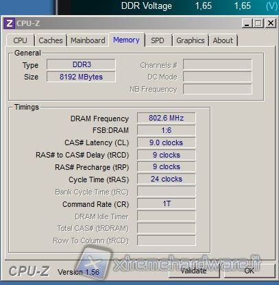
- 1600 MHz 9-9-9-24 timings
The CPU (i7 2600K) was not overclocked and its frequency has remained at default (3.4GHz), also we did not change the parameters of energy savings and those related to the Turbo Boost technology.
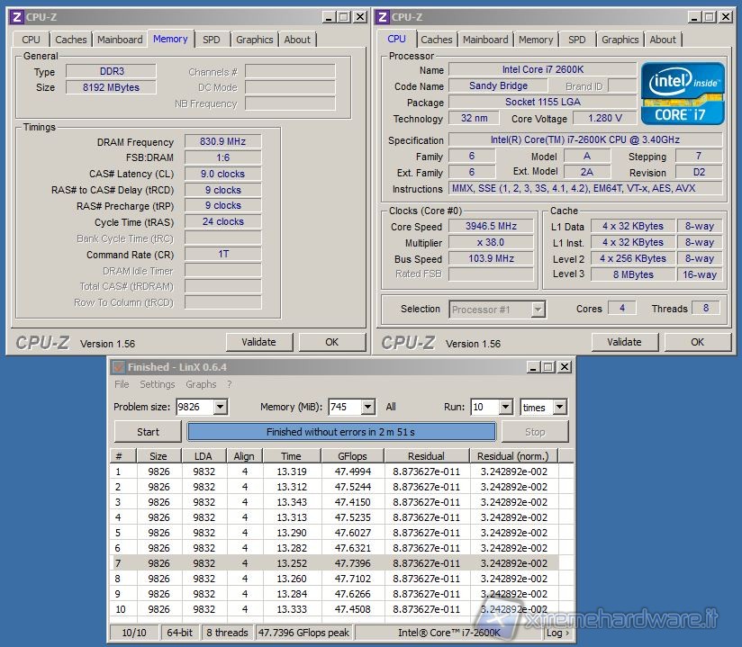
Finally, increasing the BCLK we managed to bring the RAM to 1660 MHz without changing the voltages and latencies compared to the default setting. In this case, however, the CPU frequency is increased to 3.95 GHz
It's important to note that the settings at 1333 MHz and 1600 MHz were stable even with voltages below the specifications, indeed, using these settings we were able to complete 10 cycles of Linx stress test using only 1.57 V. In addition, throughout the test session, it was not necessary to change the VCCIO voltage that was left then to 1.05 V. Recall that this setting refers to the voltage of the integrated memory controller.
As always, we remind you what we mean by access timing, whose values can be set by the BIOS of the motherboard:
- CasLatency Time (TCL): during a read operation, represents the time interval between the instant at which the read command arrives at a certain memory cell and the one at which the data transfer begin.The name is due to the fact that, to locate the memory cell, the column address is always the last selected (via the CAS signal), after the one relative to the line.
- RAS to CAS Delay Time (TRCD) is the interval of time between activation of row and column that identifies the memory cell in which you want to read or write the data, namely the delay between CAS signal and RAS signal.
- Ras Precharge Time (TRAS): represents the period of time when a certain line is active, before the coming of the precharge signal.
- RowPrecharge Timing (TRP): This BIOS setting specifies the minimum amount of time between two successive activations at the same DDR module. The shorter the interval, the faster the next bank of memory can be activated for read or write.